NOT RECOMMENDED FOR NEW DESIGNS
The ITG-3050 is a single-chip, digital output, 3-Axis MEMS gyro IC which features a 512-byte FIFO and a secondary I²C sensor bus that interfaces to 3rd party digital accelerometers. The combination of FIFO and dedicated sensor bus allows the ITG-3050 to directly acquire data from an off-chip accelerometer, without intervention from an external processor. This both lowers the traffic on the primary (application processor) bus interface, and saves power by allowing the system processor to burst read sensor data from the ITG-3050’s FIFO, and then enter a low-power sleep mode while the device collects more data.
The ITG-3050 gives users a direct upgrade path to InvenSense’s MPU and IMU family of products by connecting the 3rd party accelerometer to the ITG-3050’s secondary I²C Bus. The ITG-3050 is pin-to-pin compatible with the MPU and IMU family of products, which allow integration with InvenSense’s software solutions.
The ITG-3050 features a 3-axis digital gyro with programmable full-scale ranges of ±250, ±500, ±1000, and ±2000 degrees/sec (dps or °/sec), which is useful for precision tracking of both fast and slow motions. Rate noise performance sets the industry standard at 0.01 dps/√Hz, providing the highest-quality user experience in pointing, gaming, user interface, and other motion-based applications. Factory-calibrated initial sensitivity reduces production-line calibration requirements.
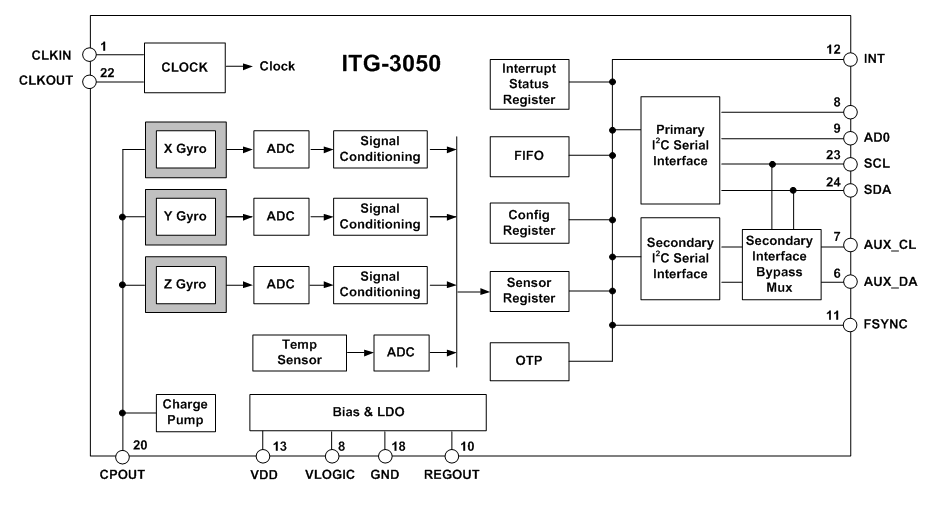
Other industry-leading features include on-chip 16-bit ADCs, programmable digital filters, a precision clock with 1% drift from -40°C to +85°C, an embedded temperature sensor, programmable interrupts, and a low 5.9 mA supply current. The ITG-3050 comes with an I²C serial interface, a VDD operating range of 2.1 V to 3.6V, and a VLOGIC interface voltage from 1.71 V to 3.6 V.
By leveraging its patented and volume-proven CMOS-MEMS fabrication platform, which integrates MEMS wafers with companion CMOS electronics through wafer-level bonding, InvenSense has driven the ITG-3050 package size down to a revolutionary footprint of 4 mm x 4 mm x 0.9 mm (QFN), while providing the highest performance, lowest noise, and the lowest cost semiconductor packaging to address a wide range of handheld consumer electronic devices. The device provides the highest robustness by supporting 10,000g shock in operation. The highest cross-axis isolation is achieved by design from its single silicon integration.
Note: The ITG-3050 is not recommended for new designs
| Part # | Gyro Full Scale Range | Gyro Sensitivity | Gyro Rate Noise | Digital Output | Logic Supply Voltage | Operating Voltage Supply | Package Size |
|---|---|---|---|---|---|---|---|
| UNITS: | (°/sec) | (LSB/°/sec) | mdps/rtHz | (V) | (V) | (mm) | |
 ITG-3050 |
±250 ±500 ±1000 ±2000 |
65.5 32.8 16.4 8.2 |
0.01 | I²C | 1.71 to VDD | 2.1 to 3.6 | 4x4x0.9 |